Smart Ring Manufacturing: The Complete Technical Guide for OEM Buyers
The smart ring market is undergoing a structural shift. What began as a niche wellness accessory has matured into a medical-grade wearable category, with hospitals, remote patient monitoring platforms, and corporate wellness programs driving procurement. For OEM buyers—whether a health-tech startup, hospital purchasing group, or electronics distributor—understanding the manufacturing architecture behind these devices separates informed sourcing from costly missteps. For deeper analysis on navigating these production partnerships, see our complete guide to smart ring OEM/ODM manufacturing.
This guide examines five engineering pillars that determine smart ring performance, manufacturability, and reliability: miniaturized electronics integration, housing material selection, sensor configuration, ingress protection, and power delivery architecture.
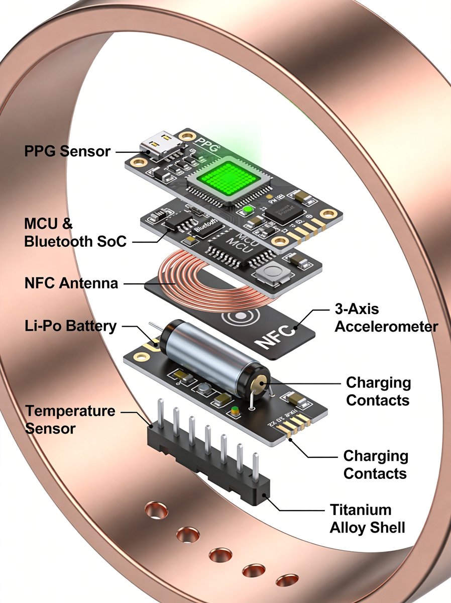
The Miniaturization Problem: Why PCB Stacking, Battery Density, and Antenna Design Define the Category
Building a smart ring is fundamentally different from building a smartwatch. A wrist-worn device offers roughly 10-15 cm³ of internal volume. A ring operates within 1.5-3.5 cm³. Every millimeter of PCB real estate, every milliwatt of power, and every fraction of a gram must be justified.
PCB Stacking: Rigid-Flex and HDI
Production-grade smart rings use a rigid-flex PCB stack: circuitry split across multiple rigid sections connected by flexible polyimide ribbons, allowing the assembly to curve along the ring’s inner circumference. This maximizes usable board area, isolates noise-sensitive analog front-ends from digital switching noise, and creates natural break points for assembly fixturing.
Most commercially viable designs use 4-6 layer HDI boards with laser-drilled microvias. Trace width and spacing drop to 3 mil (0.075 mm) or below, and via-in-pad techniques become necessary for BGA-packaged sensors and Bluetooth SoCs. For OEM buyers, the key question is whether your manufacturing partner has in-house HDI PCB capability—this dramatically shortens iteration cycles during EVT (Engineering Validation Test).
Battery: The Energy Density Ceiling
The battery is typically a curved lithium-polymer pouch cell, custom-shaped to follow the ring’s arc. Current cells achieve roughly 200-250 Wh/L, translating to 15-25 mAh. Every sensor, transmission, and LED pulse draws from this fixed budget.
Three design decisions directly impact battery life:
- Bluetooth LE PHY: BLE 5.0+ with LE Coded PHY trades data rate for link budget. Most rings default to 1M PHY for routine sync and engage Coded PHY only when signal drops.
- PPG sampling strategy: Continuous PPG at 100 Hz consumes ~3-5 mA. Duty-cycling to 25 Hz for resting heart rate and bursting to 100 Hz only during activity extends battery life by 40-60%.
- Sleep current: A well-designed ring draws under 50 µA in deep sleep, requiring careful PMIC selection and firmware-level peripheral gating.
Antenna: The Material Challenge
The antenna faces a unique adversary: the human finger. Body tissue is a lossy dielectric at 2.4 GHz. Most designs use a slot antenna cut into the inner housing surface or a chip antenna in the PCB stack, with the housing itself as part of the radiating structure. Titanium and ceramic are significantly more RF-transparent than stainless steel. If your product requires NFC, antenna co-location with Bluetooth becomes a coexistence engineering problem that must be addressed at PCB layout, not patched in firmware.
Housing Materials: Ceramic vs. Titanium vs. Stainless Steel
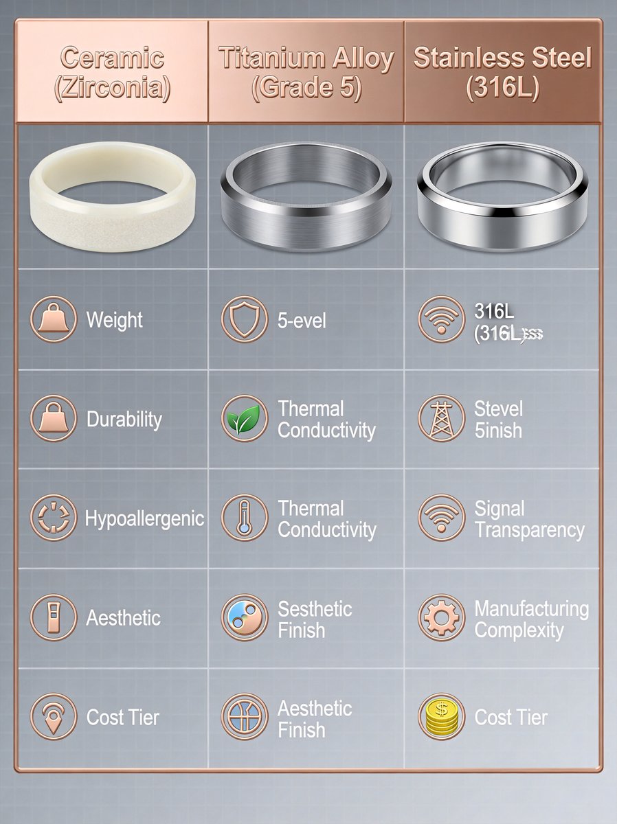
The choice of ring housing material is not primarily an aesthetic decision. It directly impacts RF performance, biocompatibility, manufacturing yield, and unit economics.
| Property | Zirconia Ceramic | Titanium Alloy (Grade 5 / Ti-6Al-4V) | Stainless Steel (316L) |
|---|---|---|---|
| Density | ~6.0 g/cm³ | ~4.43 g/cm³ | ~7.99 g/cm³ |
| Hardness | 8.5 Mohs (scratch-proof in practice) | 6.0 Mohs (scratch-resistant) | 5.5 Mohs (visible scratches over time) |
| RF Transparency | Excellent (non-conductive) | Good (conductive but low magnetic permeability) | Poor (higher loss, requires antenna tuning) |
| Hypoallergenic | Yes (bio-inert) | Yes (medical-grade) | Generally yes (nickel content varies) |
| Surface Finish Options | Glossy, matte, color-glazed | Sandblasted, anodized, PVD coated | Polished, brushed, PVD coated |
| CNC Machining Complexity | High (requires diamond tooling, post-sintering grinding) | Moderate-High (work-hardening, requires sharp tooling) | Low-Moderate (mature process) |
| Relative Unit Cost | Highest | Medium-High | Lowest |
Ceramic (Zirconia)
Yttria-stabilized zirconia (Y-TZP) offers the best combination of scratch resistance, RF transparency, and premium feel. It is also the hardest to manufacture at scale. The process involves pressing zirconia powder into a near-net-shape blank, sintering at 1,400-1,500°C, and diamond-grinding to final dimensions. Sintering shrinkage is approximately 20%, so tooling must be oversized. Early production yields rarely exceed 70-75%, though mature processes push above 90%. Ceramic suits premium positioning where RF performance (especially NFC) is critical; it is less suitable for aggressive cost targets. For OEMs prioritizing independent cellular connectivity over short-range NFC, transitioning to a 4G LTE standalone smart watch equipped with medical-grade sensors provides a robust alternative for continuous remote patient monitoring without smartphone dependency.
Titanium Alloy (Grade 5)
Ti-6Al-4V is the industry workhorse: excellent strength-to-weight ratio, naturally hypoallergenic, CNC-machinable to ±0.02 mm. Surface treatments include anodization (producing colors from bronze to deep blue) and PVD DLC coatings for scratch protection. Titanium’s main drawback is machinability—it work-hardens, generates heat, and requires carbide or diamond-coated tooling, with cycle times 2-3× longer than steel. The trade-off is a housing roughly 45% lighter than steel.
Stainless Steel (316L)
316L remains viable for entry-tier products. The machining process is mature and cost-efficient; the higher density provides a reassuring heft. The primary limitation is RF: steel’s conductivity increases eddy current losses, reducing Bluetooth range by 1-3 dB versus titanium. This is manageable with careful antenna matching but requires a larger antenna keep-out zone.
Sensor Selection: Building the Biometric Stack
The sensor suite inside a smart ring defines its market positioning. OEM buyers should approach sensor selection as a function of target use case, not as a checklist of features.
PPG (Photoplethysmography): The Core Sensor
PPG is the foundational biometric sensor. It emits green, red, or infrared light into the skin and measures the reflected signal with a photodetector—the pulsatile component corresponds to blood volume changes with each heartbeat.
Key specifications for OEM evaluation:
- Channel count: Multi-channel PPG (3-6 LED-photodetector pairs) provides redundancy against motion artifacts and improves accuracy across skin tones.
- LED wavelength mix: Green (525-535 nm) for heart rate during activity; red (660 nm) and infrared (940 nm) penetrate deeper for SpO2 estimation.
- Analog front-end (AFE): The AFE IC determines the noise floor. A 22-bit ADC with ambient light cancellation is table stakes for medical-grade accuracy.
Skin Temperature
An NTC thermistor mounted on the inner ring surface provides continuous temperature readings with ±0.1°C precision. Key applications: illness onset detection (a 0.5-0.7°C deviation from personal baseline precedes symptoms by 12-24 hours) and menstrual cycle tracking. Critical design variables: thermistor placement and thermal isolation from the heat-generating PCB.
NFC
NFC serves two purposes in smart rings. User-facing: contactless payment, access control, tap-to-connect pairing. Manufacturing-facing: a factory test interface allowing QA stations to read serial numbers, firmware versions, and calibration data without powering the ring. If your product roadmap includes NFC payment, the Secure Element certification path—discrete SE chip or embedded SE within the Bluetooth SoC—must factor into the development timeline early.
3-Axis Accelerometer
Accelerometers handle activity classification and serve as motion artifact references for PPG algorithms. The key specification is noise density: sub-150 µg/√Hz is standard for quality MEMS accelerometers. Lower noise density directly improves motion artifact subtraction accuracy.
IP68 Waterproofing: Design for Submersion, Not Just Splash
IP68 has become the de facto standard for smart rings. The rating means the manufacturer specifies depth and duration—typically 1.5 meters for 30 minutes, covering showering, hand washing, and shallow swimming.
Three sealing strategies dominate:
- Adhesive bonding: The electronics assembly is sealed to the outer shell using medical-grade epoxy or UV-cured adhesive. Most common, effective when surface preparation (plasma treatment) is done properly.
- O-ring compression: A silicone or FKM O-ring between inner and outer housing components. Serviceable but adds 0.2-0.3 mm to wall thickness.
- Overmolding: The PCB assembly is encapsulated in thermoplastic or silicone overmold before housing insertion. Most robust, least repairable.
For OEM buyers, the key question is whether the manufacturer has in-house IP68 testing—pressure chambers, dye penetration testing, thermal cycling—or outsources it. In-house testing shortens the design-verification feedback loop considerably during EVT and DVT phases.
Charging Architecture: Contact, Wireless, and the Hidden Trade-offs
Charging a device with no exposed ports requires creative engineering. Three architectures dominate:
Pogo-Pin Contact Charging
Spring-loaded pogo pins on a charging dock contact exposed pads on the ring’s inner surface. Simplest and most cost-effective. Downsides: corrosion risk from sweat and alignment requirements. Gold-plated contacts mitigate corrosion.
Wireless Charging (Qi-Based)
A miniature receiving coil captures energy via inductive coupling. Eliminates exposed contacts. Trade-off: a ring-sized coil achieves 40-55% coupling efficiency versus 70-80% for smartphone coils, meaning longer charge times and more heat.
Proprietary Magnetic Connectors
A magnetic alignment system with recessed contacts combines contact charging efficiency with magnetic docking ease. Adds component cost and custom connector tooling but delivers a premium user experience.
The charging choice cascades into industrial design. Wireless charging coils must avoid metal housing sections that shield magnetic fields, often requiring a ceramic or plastic window in the housing.
Manufacturing Partner Selection: What to Evaluate Beyond the Spec Sheet
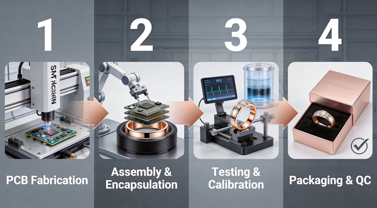
When evaluating an ODM partner for smart ring production, the conversation should move past unit pricing and MOQ to examine four structural capabilities:
1. Miniaturization track record. A manufacturer that has delivered smart rings, hearing aids, or true wireless earbuds understands the assembly challenges of sub-5 cm³ devices. One whose experience stops at smartwatches may underestimate the difficulty.
2. In-house sensor calibration. PPG sensors require per-unit calibration for LED brightness variance, photodetector sensitivity, and optical path differences from housing tolerances. A factory performing this calibration in-house—using a controlled optical phantom—delivers more consistent biometric accuracy than one relying on the sensor vendor’s factory calibration.
3. Regulatory support. Whether your target market requires CE, FCC, or medical device registration, the ODM partner should provide the technical documentation package—schematics, BOM, mechanical drawings, test reports—in the format required by the relevant notified body. They should also support factory audits for ISO 13485 or MDSAP as needed. While regulatory compliance secures initial market entry, maintaining it requires a robust post-market infrastructure. For deeper analysis, see our guide on building a global B2B after-sales and technical support network.
4. Firmware and algorithm capability. The PPG algorithm, sleep staging, and activity classifier differentiate a ring from a commodity. An ODM partner offering co-development of firmware and algorithms—or at minimum a well-documented SDK—is significantly more valuable than one delivering hardware alone.
How Xdun Medical Approaches Smart Ring ODM
At Xdun Medical, smart ring manufacturing draws on 28 years of electronics production experience and 14 years of wearable specialization. The Shenzhen-based facility handles the full chain—rigid-flex PCB design, SMT assembly, CNC housing machining, sensor calibration, and final assembly—under one roof. This vertical integration compresses the typical back-and-forth between PCB fab, housing supplier, and assembly house, which is particularly valuable during prototyping when design iterations happen rapidly.
Xdun’s engineering team has delivered smart ring projects across PPG-based health monitoring, NFC-enabled access control, and multi-sensor biometric rings. The company supports international certification requirements including CE, FCC, and FDA documentation, and accommodates both small-batch pilot runs and scaled production volumes.
For OEM buyers, Xdun offers the engineering depth to navigate the technical decisions in this guide—from material selection and antenna design through waterproofing validation and firmware integration. The cross-disciplinary team (hardware, firmware, mechanical, and quality engineering) works directly with client product teams, reducing the communication layers that slow down ODM projects.
Ready to discuss your smart ring project?
Contact the Xdun Medical ODM team for a technical consultation. Reach us at jine@xdunmedical.com or call +86-13544254314 to schedule an engineering review of your product requirements.
*This guide is provided for informational purposes. Specific manufacturing capabilities, timelines, and project scope should be confirmed directly with the Xdun Medical engineering team.*